As an emerging wide-bandgap transparent semiconducting oxide, gallium oxide (Ga2O3) is considered the fourth-generation semiconductor material surpassing silicon (Si), gallium arsenide (GaAs), silicon carbide (SiC), and gallium nitride (GaN). Ga2O3 exhibits outstanding characteristics such as high-pressure resistance and ultraviolet light responsiveness, making it of significant value in various high-performance device applications, including radio frequency devices, diodes, and solar-blind ultraviolet photodetectors.
Developed countries such as Japan and the United States have strategically positioned themselves for long-term research efforts encompassing the growth, processing, and applications of gallium oxide. The exploration of gallium oxide-related studies holds crucial significance in achieving technological leadership for China in the wide-bandgap semiconductor industry.
Associate Professor Hui Deng’s research team from the Department of Mechanical and Energy Engineering (MEE) at the Southern University of Science and Technology (SUSTech) has recently published a study that introduces a novel technology for the efficient atomic-level surface manufacturing of semiconducting oxides (see Figure 1).
Their work, entitled “Atomic-scale smoothing of semiconducting oxides via plasma-enabled atomic-scale reconstruction”, has been published in the top-tier journal International Journal of Machine Tools and Manufacture.
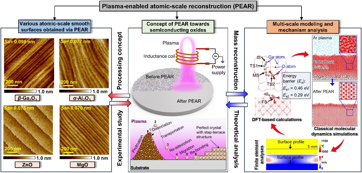
Figure 1. Graphical abstract of the paper.
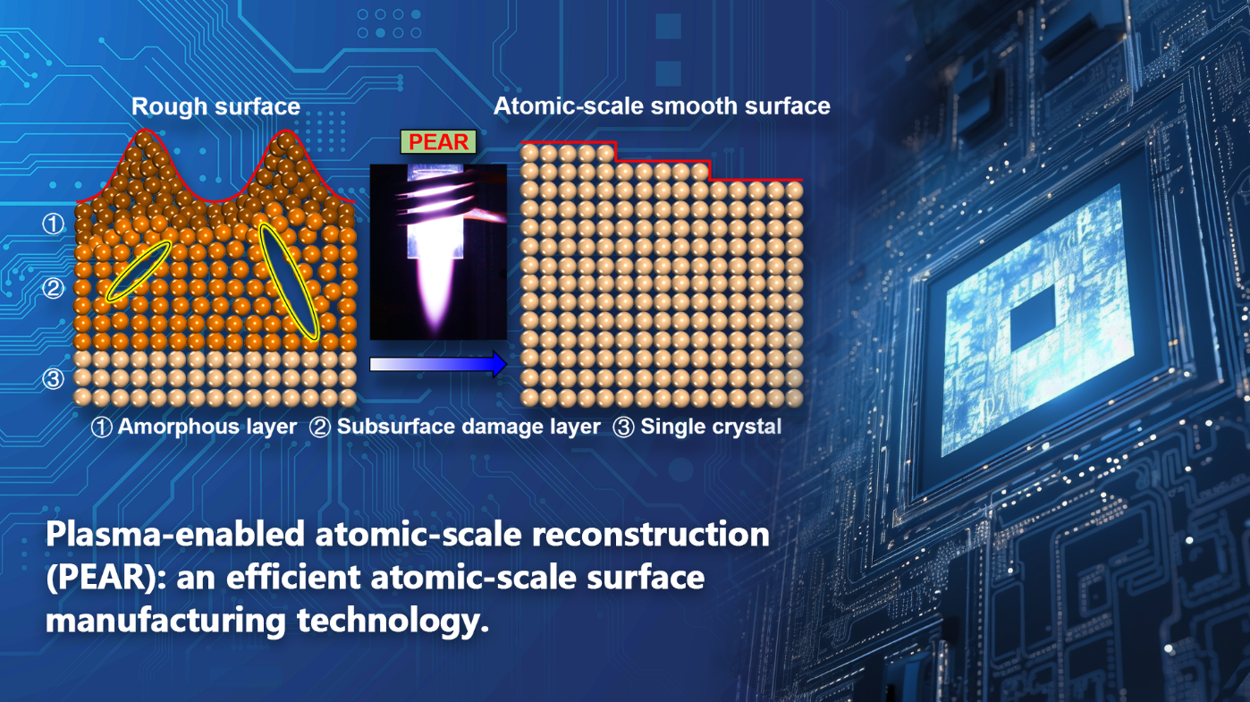
Manufacturing surfaces with atomic-scale smoothness, low damage, and regularly arranged atoms is crucial for the development of high-performance devices. Traditional methods, such as mechanical polishing or chemical-mechanical polishing, struggle to achieve high-quality surfaces that meet the requirements for manufacturing high-performance devices due to the removal principle of plastic deformation and tool action scale much larger than atomic levels. In light of this challenge, the research team proposed a novel atomic-level surface manufacturing technology tailored for semiconducting oxides. This technology, based on plasma-enabled atomic-scale reconstruction (PEAR), efficiently delivers semiconducting oxide surfaces that are not only ultra-smooth but also feature regular step-terrace structures.
Figure 2 depicts a schematic diagram of the PEAR processing applied to semiconducting oxide wafers. Through plasma scanning processing, achieving uniform reconstruction on the large-size wafer surface is anticipated (Figure 2a). Specifically, notable changes in the wafer surface and subsurface are observed before and after PEAR. At the micron scale (Figure 2b), the rough and mechanically scratched surface transforms into a smooth surface with regular step-terrace structures. At the atomic scale (Figure 2c), an amorphous layer is found on the original wafer surface, and a significant damage layer exists in the subsurface; after PEAR, the amorphous layer is recrystallized into a perfect single crystal, and the subsurface damage layer is recovered to a perfect single crystal. Figure 2d illustrates the possible principle behind the formation of the atomic-scale step-terrace surface, involving five fundamental processes: dissociation, transportation, readsorption, migration, and rebonding of surface atoms.
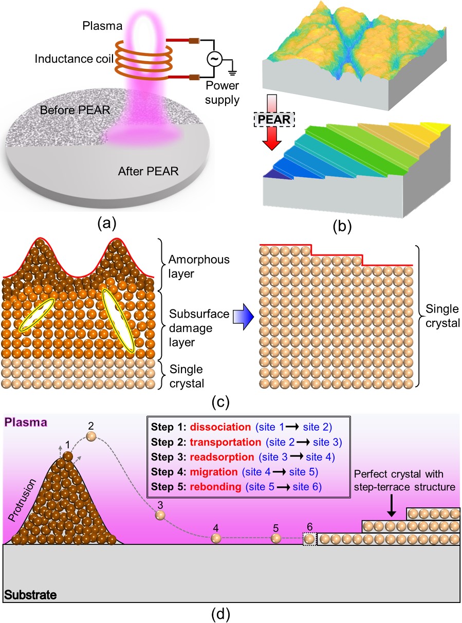
Figure 2. Schematic diagram of PEAR. (a) PEAR processing for a semiconducting oxide wafer. (b) Schematic surface morphologies before and after PEAR at the micron scale. (c) Schematic cross-sections before and after PEAR at the atomic scale. (d) Possible reconstruction process to form step-terrace structure.
Based on the aforementioned principle, the researchers conducted atomic-scale surface manufacturing studies on various semiconducting oxides, with the results illustrated in Figure 3. For the most representative β-Ga2O3, PEAR demonstrates a significant polishing effect on its different crystal faces. Similarly, for other common semiconducting oxides such as α-Al2O3, ZnO, and MgO, PEAR yields atomically smooth surfaces with clear step-terrace structures. Moreover, transmission electron microscopy results indicate that both the surface and subsurface after PEAR exhibit regular atomic arrangements without apparent atomic losses.
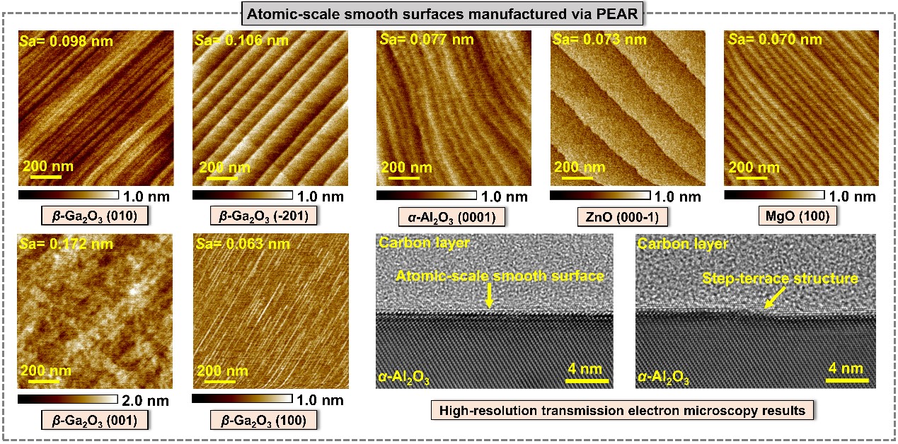
Figure 3. PEAR results for various semiconducting oxides.
The PEAR technique proposed in this study exhibits four prominent characteristics, as illustrated in Figure 4. First, PEAR involves neither material addition nor removal, making it a typical equal manufacturing process. Second, PEAR avoids any mechanical stress, enabling the fabrication of damage-free and sub-angstrom smooth surfaces. Third, PEAR enables the environmentally friendly and efficient production of surfaces with clear step-terrace structures, presenting significant advantages over traditional mechanical and chemical-mechanical polishing methods. Lastly, PEAR demonstrates excellent generality, applicable to the atomic-scale surface manufacturing of common semiconducting oxides. As a representative plasma-based atomic and close-to-atomic scale manufacturing (Plasma-ACSM) technology, PEAR holds the potential to be applied in various fields such as quantum computing, display and lighting systems, large-scale integrated circuits, and energy storage and conversion.
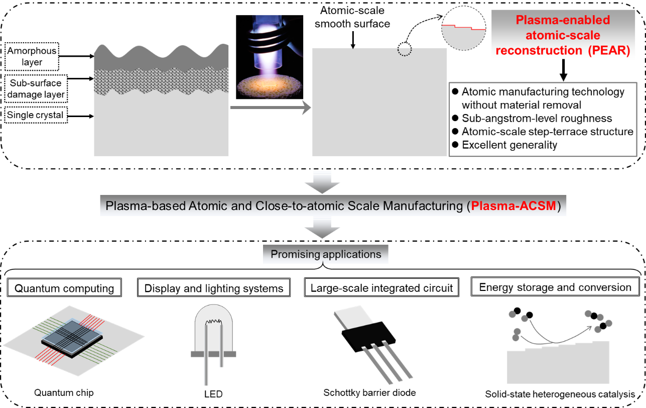
Figure 4. A summary of the outstanding features and promising applications of PEAR.
Yongjie Zhang, a fourth-year Ph.D. student from the Department of MEE at SUSTech (jointly supervised by the National University of Singapore), is the first author of the paper. Associate Professor Hui Deng is the corresponding author, and SUSTech is the first affiliated unit.
Other contributors to this study include master’s student Jin Tang and Ph.D. student Shaoxiang Liang, both of Associate Professor Hui Deng’s research team, Research Assistant Professor Junlei Zhao and Assistant Professor Mengyuan Hua from the Department of Electronic and Electrical Engineering at SUSTech, and Associate Professor Chun Zhang from the Department of Physics at the National University of Singapore.
This research was supported by the National Natural Science Foundation of China (NSFC), Development and Reform Commission of Shenzhen Municipality, and SUSTech.
Paper link: